Research: Nanoscale photoconductivity
Photoconductivity, the increase of electrical conductivity due to the absorption of electromagnetic radiation, plays the key role in photodetectors and photovoltaic devices. Rather than measuring the extrinsic photocurrent, the MIM can locally map out the intrinsic photoconductivity without the need of patterning electrodes. The spatial distribution of the photoresponse with respect to the laser wavelength and power is highly desirable for the optoelectronic material research.
Z. Chu et al. Nature Commun. 8, 2230 (2017)
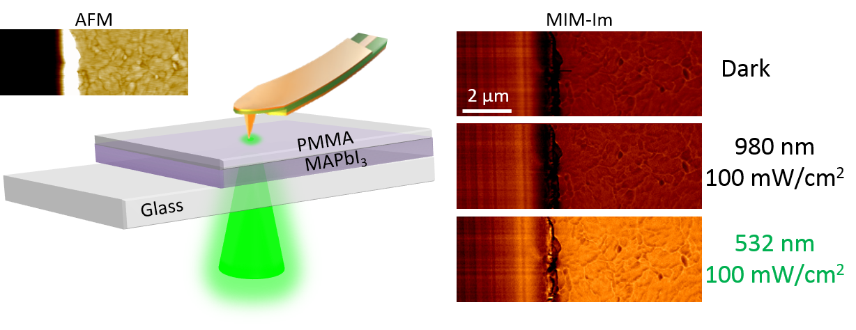
Schematic of the PMMA-coated perovskite MAPbI3 sample and the MIM setup with bottom illumination through the transparent glass substrate. The AFM image is shown on the top left corner. (Right) From top to bottom, MIM images of this sample in dark and under illumination. Clear photo response is seen when the solar cell material is illuminated by the above-gap 532-nm laser but not when illuminated by the below-gap 980-nm laser.
Y. Tsai et al. Adv. Mater. 29, 1703680 (2017)
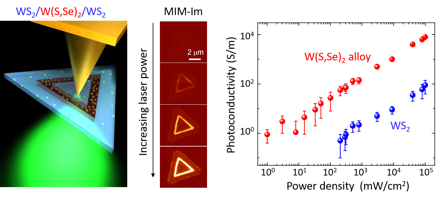
(Left) Artistic rendering of the laser stimulated MIM on the WS2/alloy/WS2 lateral hetero-junction sample. (Middle) Top-down: MIM-Im images as the laser intensity increases. (Right) Photoconductivity as a function of the illumination power. The local photoconductivity of the alloy region is enhanced by two orders of magnitude over WS2.
This research is funded by the NSF Grant EFMA-1542747 and ARO Instrumentation Grant W911NF-16-1-0276.