|
Controlled growth of nanoscale
structures on Si substrates is a forefront challenge of microelectronics.
In particular ordered organic-semiconductor interfaces are
playing increasingly important roles in fields ranging from
molecular electronics to biosensing. Successful integration
of molecular electronic devices with conventional silicon
microelectronic technology requires a detailed understanding
and control of adsorption structure in order to achieve favorable
electronic properties and ensure sufficient stability. One
example, cyclopentene molecules on Si(001) are a prototypical
organic-silicon system for which robust reversible negative
differential resistance through single molecules have been
reported. Applications in large scale circuit fabrication
of silicon-based molecular electronics, require high quality
crystals with electronic properties comparable to those of
inorganic materials. Thin organic films however cannot easily
be made by the vapor-deposition methods typically used in
microelectronics fabrication. The self-assembled growth of
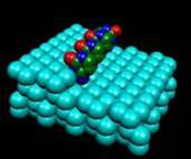
organic layers via cycloaddition on vicinal Si(001) surfaces
as templates offers a viable alternative.
While self-directed growth is more rapid than atom-by-atom
assembly, it is also less controlled, and will thus rely on
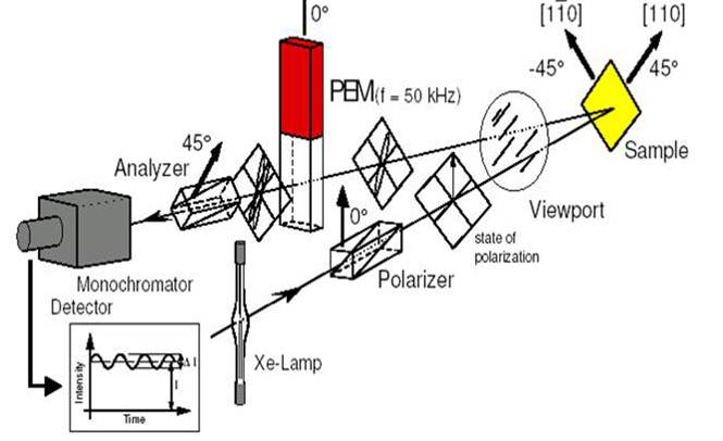
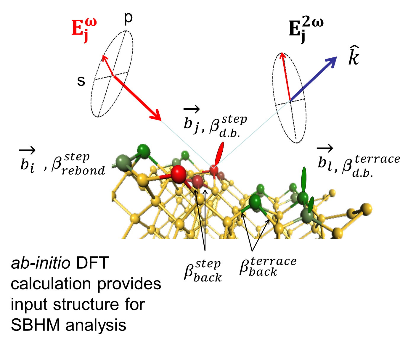
non-invasive, in-situ sensors with access to bonding configurations
at the buried interface between silicon and adsorbed nanostructure
to guide nanofabrication. Only optical techniques are able
to perform this task as routine metrology tools.
|

