Laser Spectroscopy and
Nanoparticle Research
at The University of Texas in Austin
Nanoparticle Research
at The University of Texas in Austin

NSOM
For hundreds of years the resolution of optical microscopy has been limited by the wavelength of light. Scanning Tunneling Microscopy (STM) and Atomic Force Microscopy (AFM) which have a resolution down to the atomic scale have been used successfully to investigate semiconductor structures. However, typical energy gaps in semiconductors correspond to photons with wavelength in the visible spectrum. Therefore optical microscopy and spectroscopy is useful for investigation of semiconductor structures, optoelectronic devices, and also biological samples. The problem is, that the dimensions of semiconductor structures especially quantum heterostructures are far below a micron, the approximate limit for conventional optical microscopy (400-500nm).
Near field scanning optical microscopy (NSOM) was developed in the mid 1980's as a means to break the diffraction limit on spatial resolution attainable with optical measurements. By placing a point source of light less than that distance from the sample, NSOM improves the resolution by an order of magnitude.
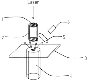
 In a traditional NSOM the light of a laser is coupled
into a single mode optical fiber (1). The fiber itself is coated with
metal (2). A scanning system (4) is moving a sample (3) relative to the
fiber while a feedback system guarantees that the distance of the fiber
tip to the surface z is in the so called optical near field range.
 A detector (6) receives reflected or transmitted light over a collection system. Detectors can be for example spectrometers or just photomultipliers. The light signal can then be analyzed in terms of intensity I(x,y) and Intensity versus wavelength I(λ,x,y). The main problem of any scanning probe microscope is to find a stable feedback system which keeps a measurable value f, as a function of the distance probe - sample z constant: f(z)=const.
A NSOM can be operated in two different modes: Illumination and collection mode (a) and Transmission and reflection mode (b). The first choice means that there is basically the possibility of illuminating the aperture and collecting the photons outside the near field (illumination mode) or doing the opposite: illuminating the whole sample and collect the photons in the near field with a small aperture (=fiber tip). In second mode (b) the reflection of the photons is opportune for opaque samples and transmission mode for transparent ones. For investigation of semiconductors quantum heterostructures a NSOM working in the collection and reflection mode is appropriate.
For feedback different techniques can be implemented to control the surface distance and reading the image. In AFM feedback the fiber tip (1) is being oscillated with a certain frequency. When the tip approaches atoms the phase of the response of the tip to the driving frequency is changed. This effect is then used to design a feedback circuit. In STM feedback is the coating (2) of the fiber tip conducting. A STM feedback can be used to keep the tunneling current constant. The NSOM images can be also recorded parallel to the AFM and STM images.