Research
Properties of materials are derived from the properties of their consituent electrons, protons, and neutrons. As a theoretical condensed matter physicist, I model macroscopic properties by starting from the basic building blocks of electrons and the nuclei to which they are bound. The properties that I am interested in are fundamental to modern technological applications. For example cell phone antennas require conversion between electronic motion and electromagnetic radiation and computer chips are increasingly depednent on a quantum mechanical description of electronic properties. My research is on the electronic and optical properties of two dimensional and nanoscale systems.
Clicking on the info buttons will give expanded text with more explanation.
Electronic properties of graphene
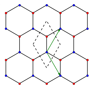
Graphene is composed of carbon atoms, shown here in red and blue, arranged in a hexagonal array. The unit cell is outlined in black dashed lines, and the lattice vectors are in green. For more information on graphene, it's relationship to graphite, and a description of unit cells and reciprocal lattice vectors, click to expand the text.
Graphite, the material in pencils, is made up of many, many layers of graphene. Weak interactions between different layers and strong chemical bonds within a layer means that it's easy for layers to peel off. This is what makes graphite a great writing tool.
The unit cell of graphene is outlined in dashed lines. This unit cell is repeated along integer multiples of the green vectors to generate the entire lattice. By breaking a macroscopic object, such as a graphene sheet, into its basic building-block (the unit cell) the problem of modeling the system is greatly simplified.
One reason that graphene is a particularly interesting system is its status as the most two dimensional object possible in a three dimensional world: it is just one atom thick. Graphene also has a high electrical mobility, meaning it is a good conductor. This property is due to a chirality of the current-carrying particles in graphene.
The most intuitive example of chirality is the existance of left and right hands. Your two hands are essentially identical, but you cannot swap the two without noticing! The concept of chirality recurs often in nature. For another example, L-glucose and D-glucose are composed of identical atoms, but the human body can only absorb one of the types, due to a different chirality. This renders them extremely different from a nutritional point of view. The electrons in graphene also have a chirality which physicists have called the pseudospin. The pseudospin of the graphene is tied to the direction of its motion: a particle moving to the right and a particle moving to the left in graphene have opposite pseudospins, which makes it hard to turn an electron around. This manifests itself as a large carrier mobility.
The large carrier mobility in graphene means there is a list of interesting physics effects that can potentially be observed for the first time in graphene. There are many other effects that have already been observed in other systems, but have previously been possible only at extremely low temperatures. This is exciting news since new technologies are more practical close to room temperature.
Optical properties of hyperbolic metamaterials
Optical properties describe how a material behaves under the influence of electromagnetic waves. The material parameter which controls this is called the dielectric function, which depends on the frequency of the electromagnetic wave, and can be used to describe transmission and reflection behavior.
Electromagnetic waves are oscillations of electric and magnetic fields. Think of a water wave, but instead of the water moving up and down, it is an electric field which gets stronger and weaker. This is where the analogy to a water wave stops working, because at the same time, a magnetic field also gets stronger and weaker. The period of a wave is the amount of time it takes for the fields to decrease from maximum, then increase again. Often we use the frequency, which is 1 divided by the period, to describe how rapidly the peaks go by. So the frequency is high if the period is short: a peak in electric field happens more often.
Light is an electromagnetic wave that happens to be just the right frequency that humans can see it with their eyes. Radio waves, infrared radiation, and ultraviolet waves are fundamentally no different then light, it's just that our eyes cannot detect them.
Electromagnetic waves can pass through some materials, and the material appears transparent. The fraction of an electromagnetic mode which passes through the material is called the transmission, which can depend on the frequency of light. When light reflects strongly off of a material, it appears shiny. How much of the electromagnetic wave is reflected and transmitted depends on the frequency, polarization, and direction of the light. All of this reflection and transmission behavior is described in the dielectric function.
At the microscopic level we can also get a different type of electromagnetic wave called a plasmon. Plasmons are electron density oscillations, and can occur in either three or two dimensions. Two dimensional plasmons are often called surface plasmons, because they occur at the surface of a material or the interface of two materials.
Hyperbolic metamaterials are nanostructured out of metallic and dielectric components in such a way as to engineer the relation between energy and wavevector to be a hyperbola.
Nanostructuring is the process of using advanced engineering techniques to combine materials that have sizes in the range of 1 to 100 nanometers. For scale, one human hair is approximately 80,000 to 100,000 nanometers wide. Many modern technologies make use of nanostructuring, processor chips in computers for example.
Alternating nanometer-sized layers of metallic and dielectric materials allows a material to seem more like a dielectric when light approaches from above, but more like a metal when light approaches from the side.
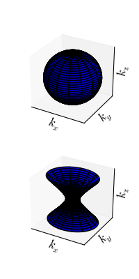
The reason for doing this is to obtain a hyperbolic metamaterial: a material which has a very special form of the frequency called a hyperbola. Given a particular frequency, the top picture is an ellipsoid. From different directions, the material might be a little easier or harder for light to pass through, but there's nothing drastic that happens. The bottom picture is a hyperbola. The surface extends far outwards along those directions, which means there are lots of electromagnetic modes available! Materials with this type of energy surface are described as hyperbolic.
The key to a microscopic understanding of the layered hyperbolic metamaterials are the surface plasmon modes at the interface of the dielectric and metallic layers. Because electromagnetic forces occur over relatively long distances (think of a magnet near the fridge) the plasmons in different layers feel one another, and form coupled plasmon modes, also known as superlattice plasmons.
In the future, it's possible that hyperbolic metamaterials could be used to create better lenses or molecular detectors.
More information
For more information about the work I have been doing, I have composed a full publication list.