Research: Novel field-effect transistors
Field-effect transistors (FETs) are of utmost importance in modern semiconductor technology. The visualization of local conductivity variation in novel FETs is expected to address many fundamental issues in electron physics, material science, and electrical engineering, including (1) real-space evolution of electronic phase transitions induced by density modulation, (2) difference between bulk chemical doping and surface electrostatic doping, and (3) microscopic origin of sub-threshold behavior in FETs.

|

|

|
D. Wu et al. PNAS 113, 8583 (2016)
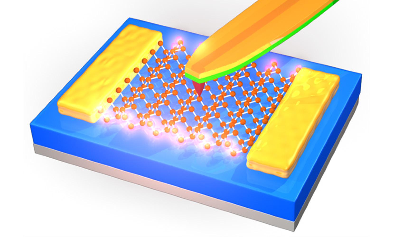
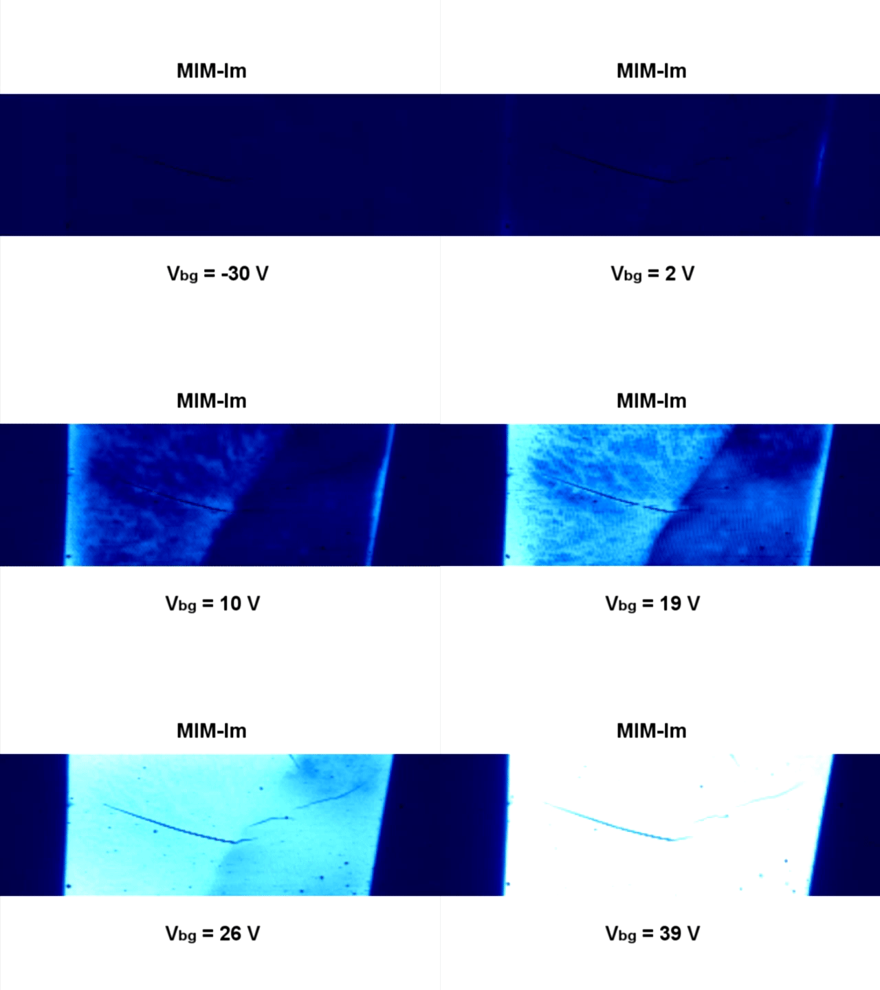
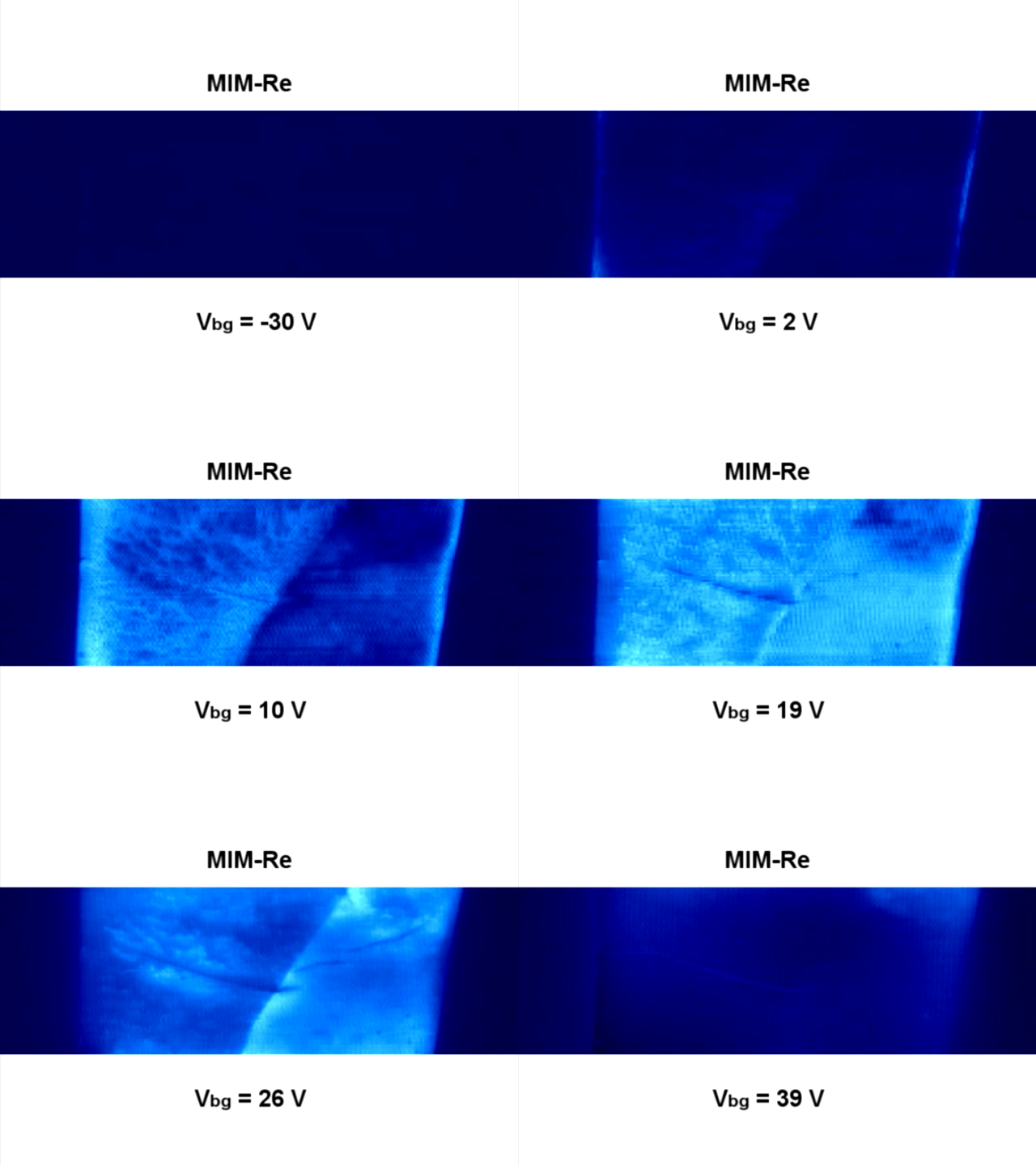
In this experiment, a back-gated FET induces the electrostatic field effect on atomically thin MoS2, a material holding high promises for the next-generation electronic and photonic devices. The MIM images with increasing back gate voltages clearly show the conductive states at the edges and thread-like electrical inhomogeneity in the interior of the sample.

Y. Ren et al. Nano Lett. 15, 4730 (2015)
Here, the ion-gel is used in the electric-double-layer transistor (EDLT) configuration on ZnO substrate. The MIM images outlined by the same color as in the transport curves demonstrate the evolution of local channel conductance acquired at 100 K.
This research is funded by the DOE under Award DE-SC0010308.