|


|
|
|
U.T. Austin Laboratory Facilities
| In our Austin laboratory, we are equipped with a wide range of surface-sensitive probes, including various forms of EELS, AES, SMOKE, XPS and LEED. These instruments operate in six Ultra-High-Vacuum chambers on the premises. |
| Thin Film Growth and Analysis Chamber |
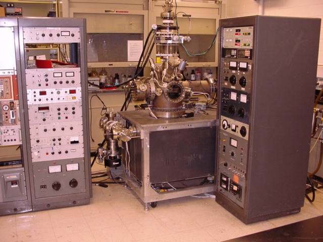 |
| Description |
| First placed in service circa 1980, this chamber incorporates double pass CMA, AES, LEED and a home-built MBE cell with ion flux and crystal microbalance film monitors. Electron beam sample heater and LN2 dewar allow sample termperature 80K - 2800K. Contact masks permit microstructure fabrication.
|
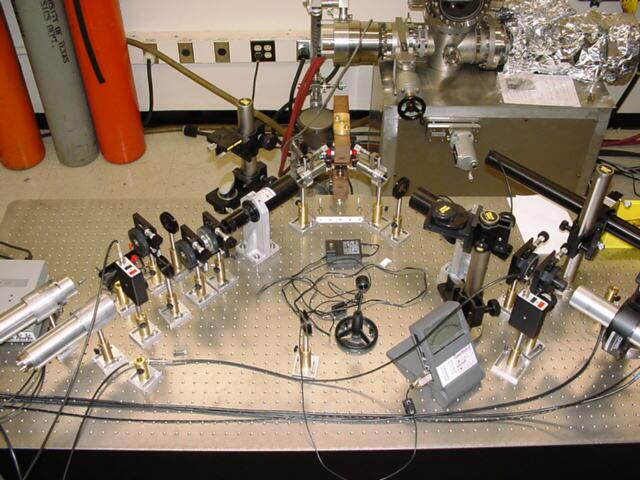
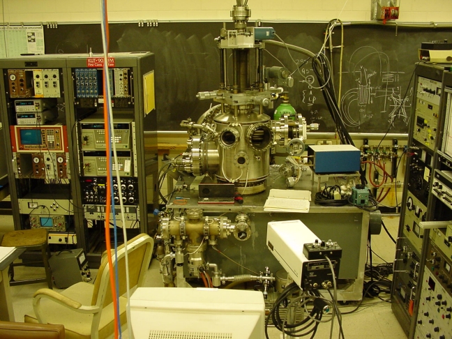
| Inelastic Electron Scattering Spectrometer |
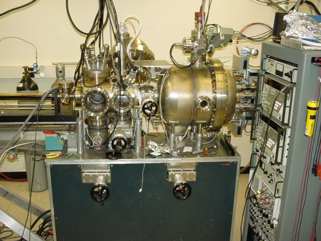 |
| Description |
| The mu-metal chamber on the right houses hemispherical analyzer based monochromator and analyzers for
performing inelastic electron scattering. The preparation chamber, (left) incorporates LEED and AES
characterization tools. |
| Inelastic Electron Scattering Spectrometer |
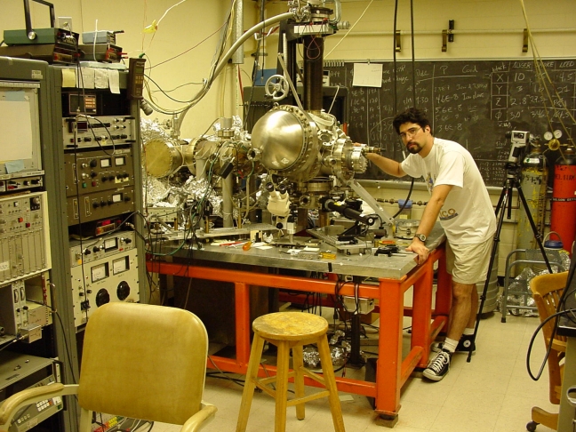 |
| Description |
| Commissioned in 1985, this chamber has been the training ground of many graduate students The system
incorporates (upper level) MBE film growth with LEED/AES characterization as well as (lower level) a MOKE
polarimeter with various magnets. The system has been used to study thin magnetic films, critical exponenets
and scaling, perpendicular anisotropy, reorientation transitions, hysteresis dynamics and surface step-induced
anisotropy.
Here, its most recent graduate, "Herr Doktor" Hector
Mireles makes preparations for growing Fe on a
continuously variably stepped W crystal as part of a study on Step-Induced
Magnetic Anisotropy. |
| SPA-LEED: Spot Profile Analysis Low Energy Electron Diffraction |
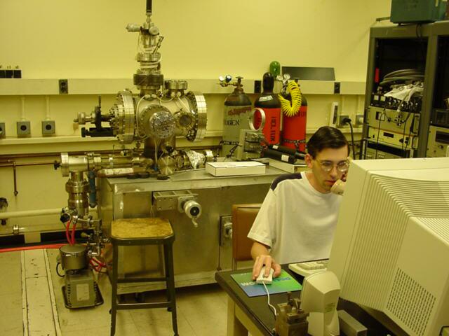 |
| Description |
| This high resolution LEED instrument includes a high transfer width electron gun, which is used in conjunction
with two MCP-RAE detector stacks. By observing the profile of individual electron diffraction spots, periodicities
on the surface, (such as monolayer steps as small as 7 Angstroms wide) can be quantitatively determined.
David Lacina, (shown here talking to Microsoft customer service) has been with the group since June, 2000. |
| High-Speed, High-Resolution Kerr Polarimeter/Microscope |
 |
| Description |
| This is a second-generation instrument for probing thin film magnetic properties that combines a long focal
length polarized light (Kerr) microscope / CCD camera with a high-speed (100 Ms/sec) Kerr polarimeter
with a small spot (few micron) focus.
The instrument is used to explore domain wall dynamics in ultra thin film microstructures. |
| High-Resolution Photoemission / Inelastic Scattering |
 |
| Description |
| This instrument incorporates film growth and characterization with LEED / AES (upper level) and a
high resolution Electron Energy Loss Spectrometer and 150 mm photoemission analyzer / Helium resonance lamp,
(lower level). Both EELS and photoemission instruments achieve 5 meV energy resolution.
The instrument is used to study shallow core level, line shapes and surface phonons. |
|
| Last Revision: Nov 20, 2005 by Jusang Yang, jsyang@physics.utexas.edu |
| Copyright ¨Ď 2005 Erskine Surface Physics Group, All right reserved. |
|
|